Your cart is currently empty!
Tag: Lithography

8-Inch SMIC Wafer CMOS Silicon Wafer Semiconductor Lithography Chip NewyI

8-Inch SMIC Wafer CMOS Silicon Wafer Semiconductor Lithography Chip NewyI
Price :27.99– 24.99
Ends on : N/A
View on eBay
Introducing the 8-Inch SMIC Wafer: The Latest in CMOS Silicon Wafer Semiconductor Lithography Chip TechnologyAre you ready for the next generation of semiconductor technology? Look no further than the 8-Inch SMIC Wafer, the latest advancement in CMOS silicon wafer semiconductor lithography chip technology. This cutting-edge wafer offers unparalleled performance and efficiency, making it the perfect choice for a wide range of applications.
With its advanced design and manufacturing process, the 8-Inch SMIC Wafer delivers superior performance and reliability. Whether you’re looking to boost the speed and efficiency of your devices or enhance the capabilities of your system, this wafer is sure to meet your needs.
Don’t miss out on the opportunity to take advantage of the latest in semiconductor technology. Upgrade to the 8-Inch SMIC Wafer today and experience the future of CMOS silicon wafer semiconductor lithography chip technology.
#8Inch #SMIC #Wafer #CMOS #Silicon #Wafer #Semiconductor #Lithography #Chip #NewyI, Semiconductor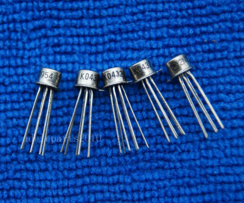
8-Inch SMIC Wafer CMOS Silicon Wafer Semiconductor Lithography Chip
8-Inch SMIC Wafer CMOS Silicon Wafer Semiconductor Lithography Chip
Price :39.00– 31.20
Ends on : N/A
View on eBay
Are you looking for top-of-the-line semiconductor lithography chips for your electronic devices? Look no further than our 8-Inch SMIC Wafer CMOS Silicon Wafer Semiconductor Lithography Chip!Our chips are designed with precision and reliability in mind, ensuring optimal performance for your devices. With advanced CMOS technology, these chips are perfect for a wide range of applications, from smartphones to computer processors.
Upgrade your devices with our cutting-edge semiconductor chips today and experience the difference in performance and efficiency. Don’t settle for anything less than the best – choose our 8-Inch SMIC Wafer CMOS Silicon Wafer Semiconductor Lithography Chip for all your electronic needs.
#8Inch #SMIC #Wafer #CMOS #Silicon #Wafer #Semiconductor #Lithography #Chip
Semiconductor Processing 3: Lithography & Etching (Semiconductor Processing Concepts)
Price: $9.99
(as of Dec 16,2024 14:50:11 UTC – Details)
ASIN : B0BZHLVVLK
Publication date : March 23, 2023
Language : English
File size : 2481 KB
Text-to-Speech : Enabled
Screen Reader : Supported
Enhanced typesetting : Enabled
X-Ray : Not Enabled
Word Wise : Not Enabled
Print length : 324 pages
Semiconductor Processing 3: Lithography & Etching (Semiconductor Processing Concepts)In the world of semiconductor processing, lithography and etching are two crucial steps that play a significant role in shaping the final product. These processes involve the precise patterning and etching of materials on a semiconductor wafer, allowing for the creation of intricate circuit designs that form the basis of modern electronic devices.
Lithography is the process of transferring a pattern onto a substrate, typically using a mask or photomask to define the desired features. This pattern is then transferred onto a light-sensitive material called a photoresist, which is coated onto the semiconductor wafer. The wafer is then exposed to light through the mask, causing a chemical reaction in the photoresist that creates a pattern on the surface of the wafer. This pattern serves as a guide for subsequent processing steps, such as etching.
Etching is the process of removing material from the semiconductor wafer to create the desired circuit patterns. There are two main types of etching: wet etching and dry etching. Wet etching involves immersing the wafer in a chemical solution that selectively removes material from the exposed areas, while dry etching uses plasma or reactive gases to etch away the material. Both methods are essential for creating the intricate features and structures that make up semiconductor devices.
Overall, lithography and etching are critical processes in semiconductor manufacturing, allowing for the precise patterning and shaping of materials on a wafer to create complex electronic circuits. By understanding these concepts, semiconductor engineers can design and produce cutting-edge devices that power our modern technological world.
#Semiconductor #Processing #Lithography #Etching #Semiconductor #Processing #Concepts
Fundamental Principles of Optical Lithography: The Science of Microfabrication
Price:$94.95– $54.72
(as of Dec 16,2024 09:40:21 UTC – Details)
Publisher : Wiley (December 17, 2007)
Language : English
Paperback : 544 pages
ISBN-10 : 0470727306
ISBN-13 : 978-0470727300
Item Weight : 1.97 pounds
Dimensions : 6.69 x 1.22 x 9.61 inches
Optical lithography is a crucial technique in the field of microfabrication, allowing for the precise patterning of structures on a small scale. Understanding the fundamental principles of optical lithography is essential for anyone working in this field. In this post, we will explore some key concepts that underpin the science of microfabrication.1. Resolution: Resolution refers to the smallest feature size that can be reliably patterned using optical lithography. The resolution of optical lithography is determined by the wavelength of the light source, the numerical aperture of the lens system, and the properties of the photoresist being used. Improving resolution is a key goal in the development of lithography techniques.
2. Contrast: Contrast is the difference in intensity between the exposed and unexposed regions of a photoresist. High contrast is essential for producing sharp, well-defined patterns. Achieving high contrast requires careful optimization of the exposure conditions, including the dose of light and the development process.
3. Depth of Focus: Depth of focus refers to the range of distances over which the image remains in focus. In optical lithography, depth of focus is limited by the wavelength of the light source and the numerical aperture of the lens system. Improving depth of focus can help to ensure that patterns are uniform across the entire substrate.
4. Overlay: Overlay refers to the alignment of multiple layers of patterns on a substrate. Achieving precise overlay is essential for creating complex structures with multiple layers. Techniques such as global and local alignment are used to ensure accurate overlay in optical lithography.
5. Resolution Enhancement Techniques: In order to improve resolution beyond the limits imposed by the wavelength of light, various resolution enhancement techniques are employed in optical lithography. These include techniques such as optical proximity correction, phase-shifting masks, and immersion lithography.
Understanding these fundamental principles of optical lithography is crucial for anyone working in the field of microfabrication. By mastering these concepts, researchers and engineers can develop innovative techniques for patterning structures on a small scale, enabling the creation of advanced microdevices and sensors.
#Fundamental #Principles #Optical #Lithography #Science #Microfabrication
